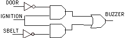
Figure 1: Schematic diagram used in the example below.
In this tutorial you will learn how to create a new project and enter a design using the Schematic Editor in the Schematic Flow mode. In later sections you will learn how to create more complicated projects using macros and hierarchies. For now let us assume you want to build a really simple circuit, as shown in Figure 1, using the Schematic Editor. This circuit will be used in a car to generate a warning signal when "The Ignition key is in the lock AND the door is open OR the seatbelt is not used". The corresponding Boolean expression is:
Figure 1: Schematic diagram used in the example below.
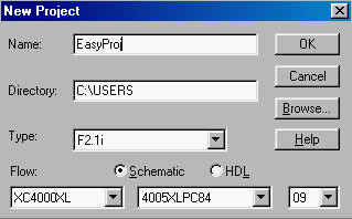
Figure 2: New Project window (Screen clip from Xilinx (TM) Foundation software)
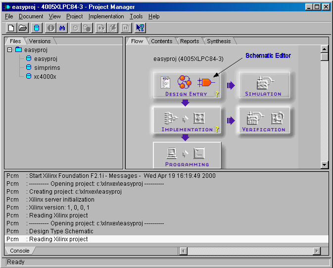
Figure 3: Xilinx Foundation Project Manager window (Schematic Design Entry) (Screen clip from Xilinx (TM) Foundation software)The project will have a .PDF extension. Other project files such as schematics, netlists, macros, etc., will be stored in a subdirectory with the project name. A project can have only one top schematic (or HDL source file). Sub-schematics can be added to the project as macros.
For more information about the Project Manager, use the online help function by selecting HELP -> PROJECT MANAGER FOUNDATION HELP CONTENTS in the Project Manager window. To access the Foundation 2.1i User Guide, go to the HELP ->ONLINE DOCUMENTATION menu. Next, click on the WEB BOOKS button and on Foundation Series 2.1i Software link.
![]()
Figure.4: Xilinx Foundation Schematic Capture window with blank schematic (Screen clip from Xilinx (TM) Foundation software)i. Placing symbols
You can add the logic symbols by clicking on the Symbol Toolbox (Symbols
icon) on the toolbar on the left. An SC Symbols Toolbox will pop up. You
can scroll down the list and select AND2 or type the symbol name at the
bottom box of the list. Notice that a brief description of the selected
symbol appears at the bottom. You can now place the gate with your cursor
on the schematic by clicking the mouse. To place another AND gate just
click on the previous one and a second gate will be attached to the cursor.
Every time you click another gate of the same type will be placed in the
schematic until you press the Escape (ESC) key.. Place two 2-input NAND
gates. Next, select OR2 from the SC Symbol Toolbox and drop one OR gate. Figure
5 shows the schematic with the symbols added.
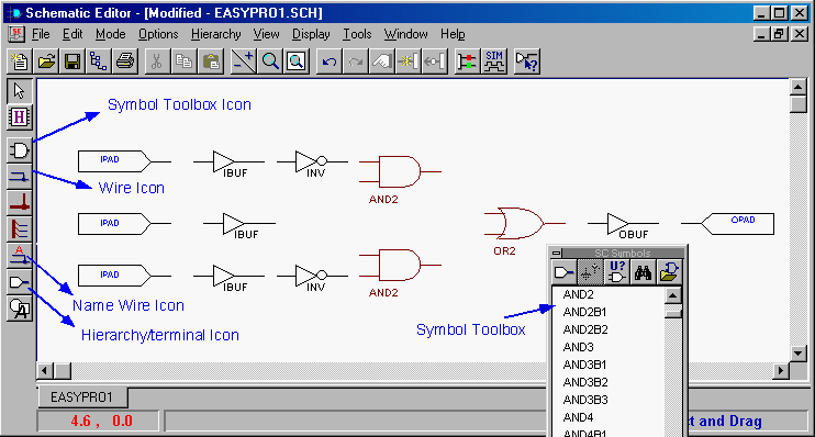
Figure 5: Xilinx Foundation Schematic Capture window with Symbols added (Screen clip from Xilinx (TM) Foundation software).
ii. Adding I/O buffers, pads and I/O terminals
FPGAs and CPLDs have input/output blocks that act as an interface between the internal circuitry and the pins which connect to the external world. The I/O block can be configured by the user. It consists of input and output buffers (designated by the library symbols IBUF and OBUF), tri-state output buffer (OBUFT) and flip-flops (edge-trigger D flip flop (IFD) or a latch (ILD)).
Buffers:
Buffers are needed for input and output signals which go to a pin of your device (FPGA or CPLD). Place the buffers on the schematic in a similar fashion as you did for the other symbols. For the input buffers select the IBUF symbol and for the output buffer select OBUF from the SC Symbol list. In case you would like to add a tri-state buffer, you can select OBUFT. Do not forget to add buffers or your schematic will not compile later on!
Pads:
You will also need to add I/O pads to the input and output buffers. These pads represent the actual pins on the XILINX device. A pad is a physical component in the Xilinx Unified Library and is placed like any other component (ex. AND, NAND, etc.). The names of pads are IPAD (input), OPAD (for output), IOPAD (bi-directional), IPAD4 and OPAD4, etc. All device pins MUST be represented with one of these I/O pads! Pads should be given a name and possibly a pin number (pin location). This can be done by double clicking on the pad to bring up the Symbol Properties window (see Adding pin locations below). Output pads are pulled-high or pulled-low through a pull-up or pulldown resistor of about 10 kOhm, respectively, when not in use to prevent floating outputs. During normal operation, the pull-up/down is deactivated.
Pins
An I/O terminal (pin: ![]() ),
which is available by clicking on the I/O Terminal button at the bottom
of the left-hand side toolbar or at the top of the SC Symbols window,
is not a physical device and cannot be used as an I/O pad (although,
sometimes the software may treat it as an I/O pad, but there is no guarantee).
I/O terminals should only be used to provide connections between
levels of hierarchy in the design. Thus they are used in macros to connect
signals to the corresponding pins on the macro symbol. However, signals
that span multiple pages of a flat design do not require terminals or off-page
connectors. To indicate device pins on the top-level schematic in
a hierarchical design, one should not use I/O terminals but pads to indicate
device pins.
),
which is available by clicking on the I/O Terminal button at the bottom
of the left-hand side toolbar or at the top of the SC Symbols window,
is not a physical device and cannot be used as an I/O pad (although,
sometimes the software may treat it as an I/O pad, but there is no guarantee).
I/O terminals should only be used to provide connections between
levels of hierarchy in the design. Thus they are used in macros to connect
signals to the corresponding pins on the macro symbol. However, signals
that span multiple pages of a flat design do not require terminals or off-page
connectors. To indicate device pins on the top-level schematic in
a hierarchical design, one should not use I/O terminals but pads to indicate
device pins.
If the schematic is going to become a cell or macro that will be used later on in a larger schematic you need to use I/O terminals to indicate the terminals of the device. As explained above you can add an I/O terminal (pin) by clicking on the Hierarchy Connector icon and entering the name of the terminal. For macros, you don't need to place buffers in the schematic (IBUF or OBUF) since the inputs and outputs will not be connected to a physical pin of the FPGA or CPLD. For macros or hierarchical design, see the section on "Macros and Hierarchical Schematics".
iii. Drawing lines and naming wires
To connect one gate to the other, use the Draw Wire feature. This can be done by clicking on the wire symbol just below the Symbol Toolbox icon of the left side toolbar. All symbols must be connected with wires.
Nets (wires) should be user-defined for readability and documentation purposes. You can name a wire by clicking on the "Name Wire Icon" just below "bus" icon on the vertical toolbar. Type in a name in the Net Name window and put the cursor over the location of the wire. Make sure you point to the wire that you want to name, otherwise the name will not be connected to anything. A shortcut to naming nets is double clicking on the net. You can now fill out the net name between the pads and buffers for the three inputs (DOOR, IGNITION AND SBELT) and the output (BUZZER). Net names should appear in blue (green names indicate that the name is not connected to a net).
You can assign pin numbers to each input and output pad. If you don't do this, the compiler will assign the pin numbers for you. There are two ways you can assign pin numbers. First, you can place the pin numbers on the schematic using the LOC or Description property. This is done by double clicking on the PAD symbol. In the pop-up Symbol Properties window (Figure 6), go to the Parameters section and enter as Parameter Name: LOC, and for the Parameter Description: P#, in which # represents the pin number as shown in Figure 6 (the letter P is required in front of the number). Click on the ADD button. To display the pin location, double click on the LOC=P44 until two diamonds appear next to it. When finished click OK.
The name can be moved by double clicking on the pad until the Symbol
Properties window appears. Select LOC=P# and select MOVE. You can now move
the pin location label around.
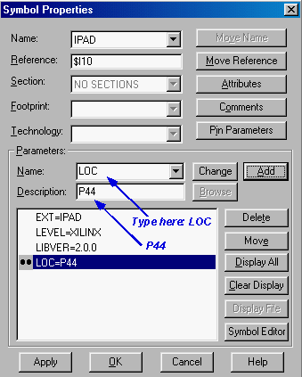
Figure 6: Symbol Properties window to assign pin locations (Screen clip from Xilinx (TM) software window)An alternative way is to not assign pins on the schematic, but specify the pin numbers later, before compiling the design. This can done by creating a User Constraint File (see constraint editor section). The advantage of the latter method is that the schematic is more generic and you can easily change pins without having to modify the schematic (or the HDL code).
When using the Digilab board, the FPGA Demoboard, the XS40, or the XS95
boards, certain pins have been pre-assigned and some are connected to LEDs
and switches for ease of testing (consult the descriptions of the Digilab
board, the Demoboard,
XS40
or the XS95 boards). Assign the
pin numbers so that you can make use of these devices. The pinouts of the
84 pin PLCC
XC4000 and
XC9500 devices are available on the web. In case you are using the
XS40 board, you can connect the inputs "DOOR", "IGNITION" and "SBELT" to
the pins of the parallel port connector (e.g. pins 44, 45 and 46, respectively
- see Table 1 of the XS40 board description) and the output to one of the
LED segments (e.g. segment "a" or pin 19). Figure
7 shows the finished schematic.
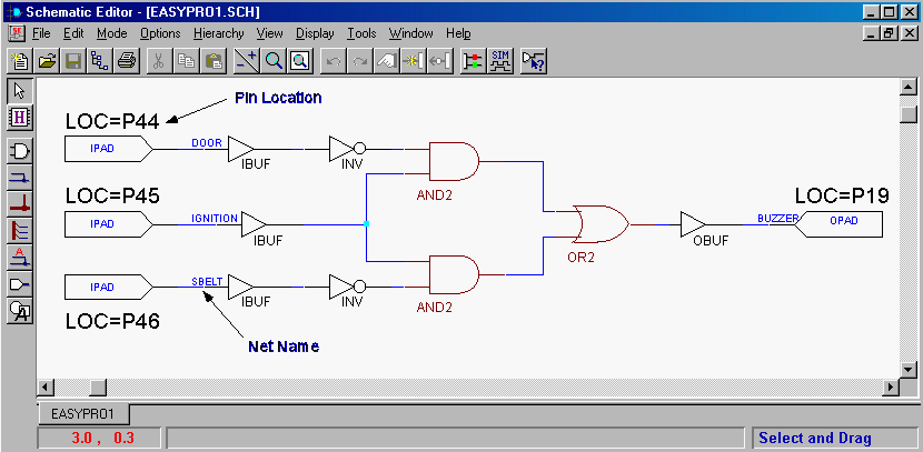
Figure 7: Schematic of the finished circuit including pin numbers locations (Screen clip from Xilinx (TM) Foundation software.v. Add your name, title of project and date
It is good practice to label the schematics clearly. There is a standard
way of doing so. Go to the bottom of the page and fill out the small rectangle.
If the box has a predefined name, you can change this by going to the FILE->TABLE
SETUP. You can now change the address, Name, Description, Date, etc.
vi. Netlist and Integrity Test
You will need to generate a netlist which is in a format that is readable by the compiler. This is done by going to the OPTIONS menu-> CREATE NETLIST. When finished, it is always a good idea to check that the schematic has no electrical design rule errors. This is done from the OPTIONS menu -> INTEGRITY TEST. You can now also generate a EDIF netlist by going to the OPTIONS menu -> EXPORT NETLIST. If you don't do this, do not worry - the system will prompt you later to do so.
Go to the FILE menu -> SAVE or click the floppy disk icon on the top toolbar. Give your schematic a name with the extension .SCH (ex. EASYPROJ.sch). When finished with the schematic, exit the Schematic capture program which will bring you back to the Foundation Program Manager window (Figure 3.3).
viii. Adding the schematic to the project
If the created schematic is not listed in the Project Manager window under the Project you created (ex. easyproj1.sch), you have to go to the DOCUMENT menu -> ADD in the Project Manager window. A window with a list of files will appear. To show only the type "Schematic" display *.SCH in the dialog window. Then select the schematic (EASYPROJ.sch) you would like to add to your project (EasyProj).
ix. Copy your project to another disk.
If you want to save your project on another disk (e.g. floppy disk) you can to do this from within Xilinx. Go to the Project Manager. Open the FILE->COPY PROJECT menu. Give the name of the Drive and directory to which you would like to copy your project.
You can also archive your project as a ZIP file. In the Project Manager,
go to FILE -> ARCHIVE PROJECT. This will open the Archive Project Wizard
window. The zip file is convenient when you need to email your project
or when the file is too large to store on a disk.
The next step is to simulate or compile (implement) the circuit.
For more information, go to the HELP -> SCHEMATIC EDITOR HELP CONTENTS menu in the Schematic Editor window. You can also read the "Design Methodologies - Schematic Flow" in the Foundation Series 2.1i User Guide. Check also the "most common mistakes" section.
References
Created by Jan Van der Spiegel <jan@ee.upenn.edu>; August 26, 1997; Updated by Jan Van der Spiegel; May 16, 2000.